
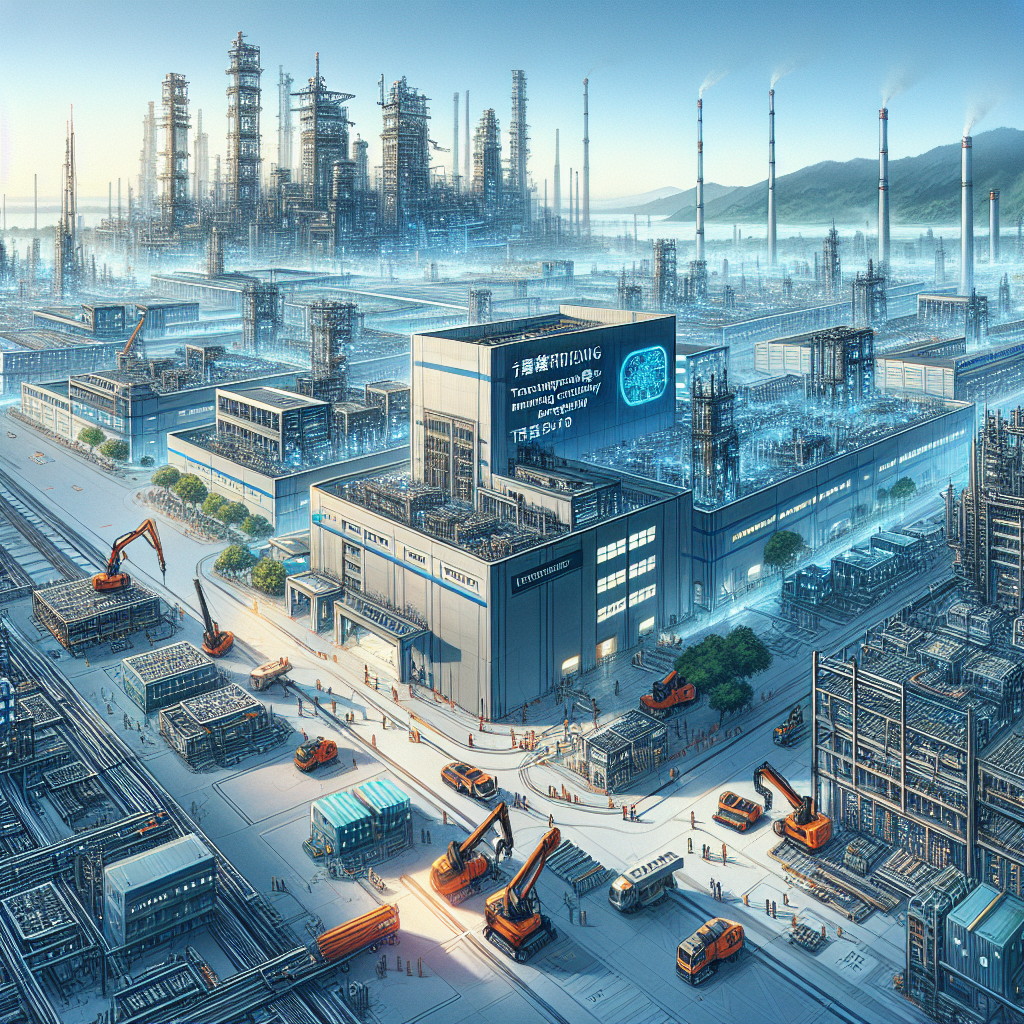
Taiwan Semiconductor Manufacturing Company (TSMC) continues to expand its investment in Kaohsiung, planning to initiate expansion projects on the east side of the P3 plant to continue advancing its manufacturing processes and leveraging the synergies of production capacity clustering. The expansion of the P4 and P5 plants is expected to commence in 2025. In addition, TSMC’s first factory in Kikuyo-cho, Kumamoto Prefecture, Japan has already begun mass production.
According to reports by the Central News Agency, TSMC has plans to construct three wafer plants in Kaohsiung, with the P1 and P2 plants producing 2-nanometer process chips. The construction planning, permit application, and on-site work for the P3 plant have already commenced, with completion and permit application expected by 2026 to produce 2-nanometer or more advanced process chips.
Due to the rapidly changing global semiconductor industry landscape, international competitive pressures, and considerations for global production process layout in the industry, TSMC has an urgent need to continuously expand its advanced process production capacity by building new plants. The expansion project is set to be continued on the land adjacent to the east side of the P3 plant.
At the public meeting for the environmental impact assessment of the expansion project, TSMC’s Vice President Zhuang Zishou mentioned that the five Kaohsiung plants are estimated to employ 8,000 employees. TSMC stated that the construction progress in Kaohsiung is being carried out in accordance with government procedures. As per the expansion plans, the construction, permit application, and on-site work for the P4 and P5 plants are expected to start in 2025, with completion and licensing scheduled for 2027.
On the 27th, Kumamoto Governor Kabaya reveals that TSMC’s first factory in Kikuyo-cho, Kumamoto Prefecture, has initiated mass production. This factory will manufacture the most advanced 12 to 28-nanometer logic semiconductors in Japan and supply them to customers such as Sony Group.
Reported by Yomiuri Shimbun and Kyodo News Agency, Kabaya disclosed this during a routine press conference. On the same day, TSMC confirmed the news, stating that “production has started as planned in December.”
The Kumamoto Prefectural Government stated that TSMC’s Japan subsidiary, JASM (Japan Advanced Semiconductor Manufacturing), notified the prefecture on the 23rd that mass production has commenced.
TSMC’s Kumamoto factory was introduced by the Japanese government to strengthen the domestic supply chain. In 2021, TSMC and Sony Semiconductor announced the establishment of a wafer plant in the region. The construction for the first factory began in April 2022, completed in December 2023, and opened in February this year, primarily producing image sensors and automotive semiconductors.
The investment in the first factory amounts to approximately 13 trillion yen (approximately 82.99 billion USD), with the Japanese government deciding to provide up to 476 billion yen (approximately 30.39 billion USD) in subsidies. The construction of the second factory is expected to commence between January and March 2025.