
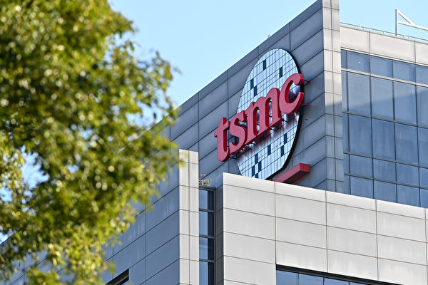
The global leading chip manufacturer, Taiwan Semiconductor Manufacturing Company (TSMC), is exploring an advanced new method for chip packaging to keep up with the demand for ultra-high computing power.
According to multiple sources familiar with the matter quoted in Nikkei Asia, TSMC is collaborating with equipment and material suppliers to develop this new method, but achieving true commercialization may take several years.
The idea behind the new method, as revealed by these sources, involves using rectangular panel-shaped substrates instead of the traditional circular wafers, allowing for more chip sets to be placed on each wafer.
This research is still in its early stages, but it signifies a significant technological shift for TSMC, which previously considered the use of rectangular substrates too challenging. To make the new method work, TSMC and its equipment suppliers must invest a significant amount of time and effort into research and development, as well as upgrading or replacing a large number of production tools and materials.
Sources disclosed that the experimental rectangular substrates currently being tested measure 510mm x 515mm, offering an available area more than three times that of a circular wafer. The rectangular shape also means there will be less unused space leftover at the edges, according to insiders.
TSMC’s advanced chip stacking and assembly technologies have been used to produce AI chips for companies like Nvidia, AMD, Amazon, and Google, utilizing the largest 12-inch silicon wafers currently available. TSMC is expanding its advanced chip packaging capacity in Taiwan to meet the growing demand. Insiders revealed that the expansion in the Taichung plant is primarily to serve Nvidia, while the expansion in the Tainan plant is for Amazon and their chip design partner, Alchip.
When asked about this, TSMC stated, “We closely monitor the progress and development of advanced packaging, including panel-level packaging.” The company declined to comment on individual customer-related issues.
Chip packaging technology was once seen as a relatively low-tech aspect of chip manufacturing, but it is becoming increasingly important in maintaining the pace of semiconductor advancements.
For AI computing chips like Nvidia’s H200 and B200, advanced chip manufacturing alone is not sufficient. TSMC’s pioneering advanced chip packaging technology, CoWoS (Chip on Wafer on Substrate), is also necessary. For example, in the assembly of B200 chips, CoWoS can combine two Blackwell graphic processors and link them with eight High Bandwidth Memory (HBM), thereby achieving high-speed data processing capabilities and significantly enhancing computational efficiency.
However, as chip sizes continue to increase to accommodate more semiconductor transistors and integrate more storage processors, the industry standard of a 12-inch wafer containing an area of about 70,685 square millimeters may soon be insufficient for efficiently packaging cutting-edge chips.
For instance, industry executives have indicated that assuming a production yield of 100%, only 16 sets of B200 chips can be produced on one wafer. Morgan Stanley estimates that approximately 29 early H200 and H100 chips can be packaged on one wafer.
“The trend is clear: chip manufacturers need to meet the demands of fast data processing, maximize chip computational power, integrate more chips, and thus increase the size of chip packaging,” a semiconductor industry executive told Nikkei Asia. “This new technology is still in the early stages of research and development. For instance, how to apply photoresist on cutting-edge chip packaging on the new (rectangular) substrates is a challenge. Chip manufacturers with strong financial capabilities like TSMC are needed to drive semiconductor equipment manufacturers to change equipment designs.”
Senior executives and analysts in the semiconductor industry say that display and PCB manufacturers are experts in handling rectangular substrates, but chip production requires higher precision equipment and materials.
Mark Li, a semiconductor analyst at Bernstein Research, stated that TSMC may need to consider utilizing rectangular substrates sooner rather than later, as AI chip assemblies will require accommodating more chips per package.
“This shift will require a large-scale overhaul of facilities, including upgrading robotic arms and automated material handling systems to deal with substrates of different shapes,” Li said. “This could be a long-term plan spanning 5 to 10 years, not achievable in the short term.”
Intel is also exploring panel-level packaging in collaboration with suppliers, and Samsung, known for its expertise in display manufacturing, is also experimenting with new chip packaging methods.