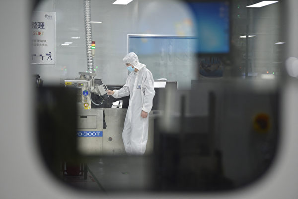
In September, the Ministry of Industry and Information Technology of the Chinese Communist Party (CCP) released the “Guidance Catalog for the Promotion and Application of the First Major Technical Equipment (2024 Edition),” which attracted attention primarily for two lithography machines listed. One of the lithography machines specified in the catalog uses a 193nm wavelength and an ArF light source with a lithography accuracy below 8nm, capable of achieving a resolution of 65nm on a 12-inch wafer.
Some mainland Chinese public opinion initially believed that the domestic lithography machine had made a significant breakthrough. Some even mistakenly thought that with lithography accuracy below 8nm, it could produce 8nm chips.
Lithography accuracy, as an essential technical indicator for lithography machines, refers to the alignment precision between each exposure layer. In the chip manufacturing process, multiple exposure patterns are stacked layer by layer on a wafer, requiring precise alignment between each layer, which is the lithography accuracy.
According to Brad Liao, a senior IC design manager in Taiwan, lithography machines use a similar exposure method to transfer patterns onto wafers. Each wafer typically produces at least 10 to 20 layers of masks, and aligning each mask with another layer involves errors due to precision deviations, known as lithography accuracy.
The domestically exposed 65nm resolution DUV lithography machine, as reported by mainland chip intelligence, is an improved version of the previous Shanghai Microelectronics 90nm resolution domestic lithography machine. It can only meet the manufacturing needs of 55-65nm mature process chips, far from reaching the 28nm process.
An industry expert revealed to chip intelligence that while the lithography machine’s lithography accuracy is ≤8nm as per factory standards, processing the wafer would introduce errors, likely resulting in around 11-12nm of lithography accuracy on products. Single exposures can achieve a maximum of 55-65nm resolution, highlighting the limitations for multiple exposures with lithography accuracy of 8nm.
Brad Liao explained that a resolution of 65nm can only achieve around 65nm at best, with the finest lines reaching approximately 65nm. ASML, a company capable of 28nm lithography, requires lithography accuracy of below 3.5nm, indicating the advanced capabilities necessary for 28nm processes.
The gap between this domestic lithography machine and international advanced standards is significant. ASML’s dry lithography machine XT:1450 launched in 2006 already achieved a 57nm resolution and 7nm lithography accuracy, highlighting an over 18-year performance difference compared to the domestic machine.
Notably, this lithography machine remains a dry DUV lithography machine, not the more advanced immersion DUV lithography machine.
Immersion lithography theoretically appears feasible but poses significant engineering challenges in practice. Referred to as the “father of immersion lithography,” Lin Benjian faced substantial difficulties during its development, reflecting the complex nature of implementing immersion lithography technology.
The data released by the Ministry of Industry and Information Technology did not specify the manufacturers of these machines or their wafer production capacity per hour. Industry insiders in China have not yet reported seeing this lithography machine.
In early September, the Netherlands Trade and Development Minister, Reinette Klever, announced changes in the country’s export controls, requiring ASML to apply for permits to sell its 1970i and 1980i immersion deep ultraviolet (DUV) lithography machines to Chinese customers.
The Dutch government stated that ASML also needs to apply for service permits to provide spare parts and software updates for previously sold immersion lithography systems to Chinese customers, which are now restricted.
In March of this year, the Netherlands already imposed export controls on the most advanced immersion DUV systems shipped to mainland China, including TWINSCAN NXT:2000i and TWINSCAN NXT:2050i.
With no access to the most advanced EUV lithography machines, DUV technology is considered crucial for China’s breakthrough in high-end chip key processes. Restrictions on such equipment may severely impact China’s chip industry.
Brad Liao explained that once the 1970i and 1980i are banned, mainland China’s technology would likely regress to at best a 65nm stage, potentially reverting to 90nm. While double exposure can allow further progress, the yield rate could drop to at least below 50%.
In mainland China, many technologies, such as automotive chips and Yangtze storage memory, rely on 28nm processes. If the 1970i and 1980i are banned, all their 28nm products will be impacted. The halt in advanced technologies could set them back five to ten years.
Starting over or purchasing from abroad would be the only options, but transitioning from one IC to another involves extensive revalidation, causing significant challenges. Brad Liao emphasized the significant impact the new ban could have on China’s chip industry.

